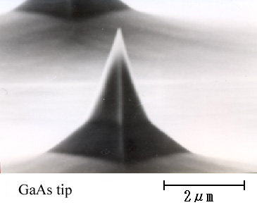
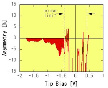
4.Development of Spin-Polarized Scanning Tunneling Microscopy
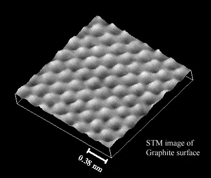
Scanning probe microscope (SPM) is a powerful tool to analyze and manipulate the nanostructures. In Yamaguchi
lab., development of a new SPM system has been tried to get some information concerning surface spin structures
and magnetic domains with an atomic scale. Recently, spin-dependent tunneling signal has been successfully
detected by a newly developed STM system using the semiconductor microtip.
Related Papers:
T.Miura and K.Yamaguchi : “ Spin-Polarized Scanning Tunneling Microscopy Using Optically Pumped GaAs Tips “, Jpn. J. Appl. Phys., Vol.41, No.6B (2002) pp.4382-4384.
篠原亮一, 山口浩一: “円偏光励起GaAsマイクロ探針のスピン偏極トンネル電子源への応用”, 電子情報通信学会論文誌 C-Ⅱ, Vol.J83-C, No.9 (2000) pp.835-841.[in Japanese]
K.Yamaguchi, R.Shinohara and M.Hashimoto : “ Spin-Polarized Scanning Tunneling Microscope Using Optically Pumped GaAs Microtips “, Functional Materials, Vol.6 No.3 (1999) pp.575-579.
Y.Suzuki, W.Nabhan, R.Shinohara, K.Yamaguchi and T.Katayama : “ Spin-Sensitive Scanning Tunneling Microscope Using GaAs Optically Pumped Tips “, J. Magnetism and Magnetic Materials, Multilayers, Vol.198-199 (1999) pp.540-544.
W.Nabhan, Y.Suzuki, R.Shinohara, K.Yamaguchi and E.Tamura : “ Effect of Dichroism in the GaAs-Tip-Based Spin Polarized STM “, Appl. Surf. Sci., Vol.144-145 (1999) pp.570-574.
R.Shinohara, K.Yamaguchi, Y.Suzuki and W.Nabhan : “ Fabrication of GaAs Microtips and Their Application to Spin-Polarized Scanning Tunneling Microscope “, Jpn. J. Appl. Phys., Vol.37, No.12B (1998) pp.7151-7154.
K.Yamaguchi and S.Tada : “ Fabrication of GaAs Microtips for Scanning Tunneling Microscopy by Wet Etching “, J. Electrochem. Soc., Vol.143, No.8 (1996) pp.2616-2619.
K.Yamaguchi, K.Okamoto and S.Yugo : “ Scanning Tunneling Microscope with Gallium Arsenide Microtip Fabricated by Selective Epitaxial Growth “, J. Appl. Phys., Vol.77, No.11 (1995) pp.6061-6063.